Combinatinal circuit output depends only on current input
We want circuits that produce output depending on current and past input values (circuit with memory)
Latcehs and Flip-Flops
- very fast, parallel access
- very expensive (1 bit cost tens of transistors)

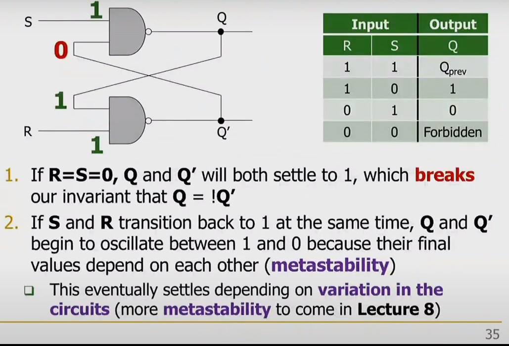
we want to prevent forbidden state in the first place.

D latches use Write enable we can prevent forbidden state issue, but more expensive.
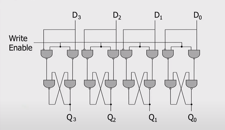
Register with D latches (multiple bits)

a singe write enable signal for all latches for simultaneous writes
Memory

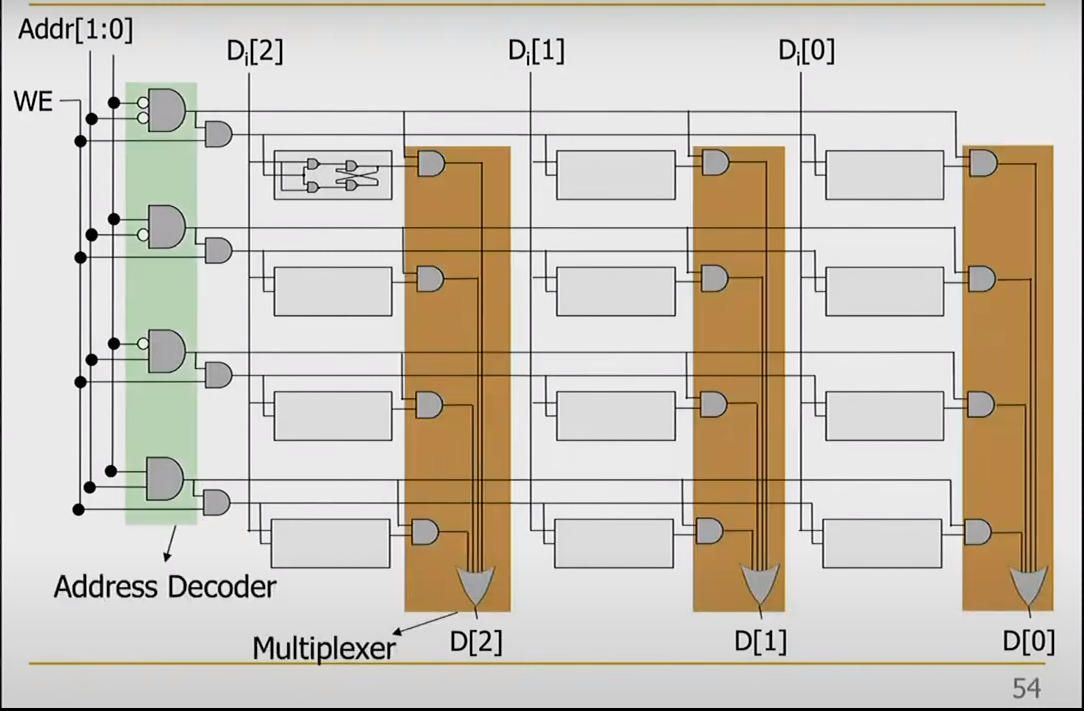
we have total 4 locations of memory array , entier set of unique location is called address space
Addressability = the number of bits of information stored in each location this case 8bits

example of 4 locations , addressability of 3bits.
2 to 4 decoder since we have 2 bits to represent 4 location , 4 to 1 multiplexer.
Clock
- general mechanism that triggers transition from one state to another in a sequential circuit
- Clock syncronizes state changes across many sequential circuit elements
- Combinational logic evalueates for the length of the clock cycle
- Clock cycel should be chosen to accommodate maximum combinational circuit delay
Finite State Machines (FSM)
A discrete time model of stateful system
- finite number of states external inputs , external outputs
- explicit specification of all state transitions
- explicit specification of what determines each external output value
Sequential circuits
State register = store the current state , load the next state at the clock edge

notice output only get affected when input is changed during the beginning of clock cycle.

we don't want this behavior , we want to change happen only at the beginning of cycle.

when enable is zero latch preserve previous value.
when clock is low D is stored in master. then when clock is high Master's D value gets written in Slave's Q
FlipFlop is edge triggered state element
plain latch is level triggerd state element
each NAND gates has 4 transistors , now D Flip Flop has over 40+ transistors.


it is D Flip Flop using clock to syncronize 4 FlipFlop.

Moore FSM = outputs depend only on the current state
Mealy FSM = outputs depend on the current state and the inputs

example of Mealy FSM , X means its value doesn't matter

outputs (lights) are not dependent on input it is soley dependent on current input which is Moore FSM.

trying to dectect pattern "1101" with Moore and Mealy FSM.
notice Mealy FSM has less state but directing output is harder than Moore FSM since Moore can just look at the state.
FSM Design Procedure
- Determine all possilble state of your machine
- Develop a state transition diagram
Static Ram (SRAM)
- relatively fast , only one data word at a time
- expensive (1 bit costs 6+ transistors)
Dynamic RAM (DRAM)
- Slower , one data word at a time , reading destorys content (refresh) , needs special process for manufacturing
- Cheap (1 bit costs only one transistor plus one capacitor)
Other storage (flash memory , hard disk ,tape)
- Much slower , access take a long time , non - volatile
- very cheap
'Computer Architecture > C.A (ETH Zürich, Spring 2020)' 카테고리의 다른 글
| Lecture 8: Timing & Verification (0) | 2021.06.11 |
|---|---|
| Lecture 7b: HW Description Lang. & Verilog (0) | 2021.06.08 |
| Lecture 5: Combinational Logic 2 (0) | 2021.06.04 |
| Lecture 4: Combinational Logic 1 (0) | 2021.06.03 |
| Lecture 2b: Mysteries in Comp. Arch. (0) | 2021.06.02 |